In-Depth Analysis of Key Chip Packaging Processes and Related Servo Hot Press Technologies
Chip packaging, as a crucial back-end process in semiconductor manufacturing, serves to protect integrated circuits from heat, moisture, and mechanical stress. It also enhances the structural integrity between functional blocks, ensuring the performance of semiconductor devices. This article focuses on three advanced packaging technologies that drive improvements in interconnects, 3D integration, and miniaturization: Flip Chip Bonding, 2.5D/3D Integration, and High-Density Interconnects (HDI).
1. Flip Chip Bonding
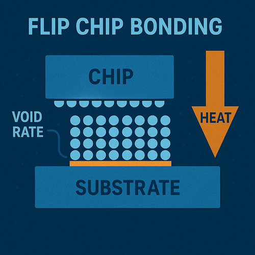
Flip chip bonding is a core interconnect technology in advanced packaging. By forming an array of solder or copper pillar bumps on the chip's I/O pads and flipping the chip to directly bond it with the substrate using thermo-compression, it replaces traditional wire bonding to achieve electrical and mechanical connection. This method reduces signal transmission length by over 80%, significantly lowering parasitic inductance (<0.1nH) and resistance (<0.05Ω).
Core Process Steps:
Bump Formation: Solder-based or copper pillar bumps are fabricated on chip I/O pads.
Alignment and Placement: The flipped chip is aligned with substrate pads.
Thermo-Compression Bonding: Heat and pressure are applied to melt the bumps and form Intermetallic Compounds (IMC).
Underfill: Epoxy resin is injected and cured to enhance mechanical strength and relieve thermal stress.

Flip Chip Bonding
Production Challenges:
Low Yield at Fine Pitch (<5μm): Thermal expansion coefficient mismatch causes stress concentration at solder-substrate interfaces, leading to solder joint cracking (batch yield<95%).
Signal Integrity Loss: Uneven pressure distribution leads to bump height deviation (>±1μm), increasing void formation (>2%) and degrading high-frequency signal transmission.
XIRO Servo Hot Press Solution
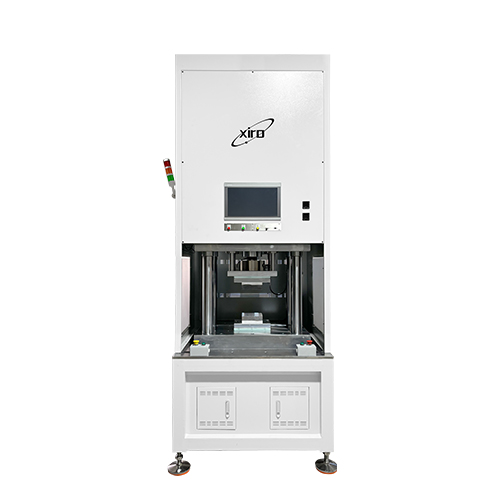
XIRO's servo hot press systems feature independently controlled upper and lower heating zones with closed-loop position and force feedback. By dynamically adjusting pressure and temperature fields, they enable uniform bump deformation and consistent IMC formation.

XIRO Servo Hot Press
Key Technical Advantages:
Gradient Pressure Control to Suppress Warpage:
Multi-zone thermal control (ΔT<1°C)
Servo-driven pressing with gradient pressure application: Preload 5MPa → Peak 30MPa → Hold 10MPa
Bump collapse height deviation <±0.5μm, improving="" solder="" joint="" yield="">99.9%
Uniform Pressure Distribution:
Stable contact resistance<0.5mΩ
Void rate reduced to<0.5%
Low-Temperature Nano Silver Sintering for Thermal Management:
Precise thermal control at 180–250°C
Efficient sintering of 20nm silver particles for high thermal conductivity (>300W/m·K)
Prevents TSV damage
2. Multi-Layer Stacked Packaging
Multi-layer stacking integrates multiple flip-chip bonded dies into a vertical 3D structure, increasing spatial utilization by 200% and reducing signal delay by 50%.
Core Process Steps:
TSV (Through-Silicon Via) Drilling and Copper Filling
Low-Temperature Bonding and Stress Compensation
Production Challenges:
Thermal Stress Delamination:
CTE mismatch between silicon and organic substrates causes interfacial delamination (warpage >1mm)
Shear strength degradation >30%
Signal Crosstalk:
TSV and RDL impedance fluctuation >10%
Signal insertion loss >0.15dB/mm at 112Gbps
Low Yield in High-Precision Stacking:
8+ layer stacking requires chip thickness ≤20μm and bonding accuracy ±0.3μm
Yield<90%
XIRO Servo Hot Press Solution
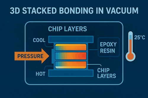
Used in HBM and 3D NAND packaging, XIRO's solution enables resin filling under vacuum and pressure gradient bonding to reduce warpage and support 12+ layer stacking.

3D Stacked Bonding in Vacuum
Key Technical Advantages:
Multi-Dimensional Optimization:
Turbo molecular pump and cryo-trap system maintain vacuum at 10⁻³ Pa
Pressure curve: 5MPa → 50MPa → 8MPa
Epoxy (viscosity<500cP) injected under vacuum to eliminate bubbles
TSV void rate<0.3%, layer warpage <10μm
Synchronous Multi-Chip Bonding:
4–8 chips bonded simultaneously
Independent thermal zones (ΔT <±2°C)
Optical alignment resolution of 0.1μm
2× higher throughput, yield >99.95%
3. High-Density Interconnect (HDI)
HDI is a core technology for advanced chip packaging, using RDL and micro-bumps (Cu Pillar) to achieve ≤2μm line/space interconnects. It supports sub-5nm nodes and enhances system-level performance.
Core Process Steps:
Microvia Drilling (Laser) and Copper Plating
Layered Insulation and Conduction Stacking
RDL via Lithography and Electroplating
Production Challenges:
Dielectric Uniformity Issues: Low-Dk materials (Dk<3.0) with="">5% thickness variation cause impedance shifts and signal reflection (insertion loss >0.1dB/mm @ 56GHz)
Microvia Plating Voids: Via holes ≤50μm suffer from >1.2% plating void rate
EMI Sensitivity: For 112Gbps PAM4 signals (28GHz equivalent), microvia and dielectric consistency must meet stringent RF standards
XIRO Servo Hot Press Solution
For edge bump arrays and high-density pads, XIRO provides localized temperature-pressure optimization to relieve CTE-induced stress.
Key Technical Advantages:
Pressure-Temperature Curve Optimization:
RDL/microvia impedance fluctuation<5%
Insertion loss reduced to 0.08dB/mm @ 56GHz
Zone-Based Independent Heating:
PID thermal compensation prevents edge damage
Dk fluctuation<1.5% for low-Dk materials
Shielding Layer Embedding:
Bonding at 250°C with controlled pressure zones ensures roughness<Ra 0.1μm, contact resistance <5mΩ
Alternating shielding-dielectric stacks form hybrid “reflect-absorb” EMI barriers, reducing leakage by >80%
4. Case Study: Ultra-Thin 48MP CIS Stacked Package
1. Thermal Stress and Warpage Control
For 16-layer 3D NAND, copper (CTE=17ppm/°C) vs. silicon (CTE=4ppm/°C) mismatch causes shear stress >60MPa, microcrack growth, and warpage >120μm/m.
XIRO Solution:
Three-zone gradient heating: 220°C (core) → 150°C (transition) → 80°C (cooling)
Temperature fluctuation ≤±0.5°C; warpage reduced to<15μm/m
Dynamic pressure compensation: 0–40MPa, accuracy ±0.3%; interface stress<25MPa
2. Ultra-Thin Chip Stacking Precision
At 35μm chip thickness, traditional alignment errors (±2μm/layer) cause total offset >32μm, TSV misalignment >8%.
XIRO Solution:
6-axis alignment: X/Y/Z ±0.25μm; θx/θy/θz ±3μrad
Laser interferometer (1kHz sampling): TSV misalignment<0.5%
3. Nano-Silver Sintering Densification
Traditional silver paste: >5% porosity, thermal conductivity<200W/m·K
XIRO Solution:
Stepwise pressurization (0.5 → 3MPa) reduces porosity<1.2%
Thermal conductivity increased to 280W/m·K
Conclusion
XIRO servo hot press systems offer advanced, precision-controlled solutions across flip chip bonding, multi-layer stacking, and high-density interconnects, overcoming challenges in signal loss, delamination, and ultra-fine integration. These capabilities position XIRO as a key enabler of high-reliability, high-yield, high-density advanced packaging.
Discover how XIRO Electric servo press technology can help your production line reduce scrap, accelerate changeovers, and improve traceability. Contact us or visit YouTube channel to explore 100+ servo press applications demos across the automotive, aerospace, and precision manufacturing sectors.


